
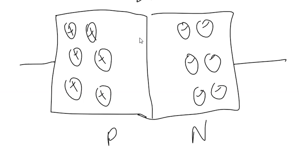
P Type Semiconductor
‘P’ type semiconductor: Silicon is doped with acceptors (e.g. Boron or Aluminium atoms (of Group III of in Periodic Table), with 1 electron less compared to Silicon) This creates a half vacant bond with silicon.
Mobile Positive Charge: ‘the Hole’
The half vacant bond of the donor atom can easily accept an electron from an adjacent silicon atom. The donor Boron atom will then be a fixed negative charge. The silicon that gives this electron has a ‘hole’ or equivalent positive charge. This hole again can accept an electron from an adjacent silicon. Thus the hole is mobile from one silicon atom to atom. This constitutes a mobile positive charge.
* Boron tends to accept electrons then become negatively (-) charge
N Type Semiconductor
‘N’ type semiconductor: Silicon is doped with donors (e.g. Phosphorus atoms (of Group V of in Periodic Table), with 1 electron more compared to Silicon.
Mobile Negative Charge: ‘Free electron’
This phosphorous atom releases easily an electron that is mobile. The donor Phosphorous atom will then be a fixed positive charge. The released electron will be mobile in the material and constitutes a negative mobile charge.
Minority Carriers:
Silicon Atoms also generate mobile charges in small numbers as electrons leave a covalent bond giving rise to a Hole-Free Electron Pair.
* Prosphorus then to release electrons then become positively (+) charge
Concentration Notations:
pp: The Holes at the p-type are majority carriers.
np: The Electrons at the p-type are minority carriers. Its concentration is denoted as: np.
nn: The Electrons at the n-type are majority carriers. Its concentration is denoted as: nn.
pn: The Holes at the n-type are minority carriers. Its concentration is denoted as: pn.
Intrinsic Carrier Concentration:
Pure Silicon can also generate hole-electron pairs due to thermal agitation. This produces holes and electron concentrations which we name as intrinsic:
ni : intrinsic electron concentration
pi : intrinsic hole concentrationSince the number of holes produces is the number of electrons released, we have ni=pi.
Commonly accepted values of ni at T = 300°K for silicon is : ni=pi=1.5 x 10¹⁶ m-3
The production of these pairs will depend on the thermal energy, thus, the Temperature; thus the growth rate will be denoted as G(T). G(T) is expected not to depend on doping.
The holes and electrons also recombine at a rate R. This will be the same as the growth rate at equilibrium (i.e. no change in ni and pi): R=G(T).
Law of Mass Action: n.p=ni2
The recombination rate R is also determine by the likelihood of a hole ‘meeting’ an electron. R will thus be proportional to the concentrations of holes and electrons. We can thus write in equilibrium for the intrinsic semiconductor without doping (pure silicon):
R=k.ni.pi=G(T) or R=kni2=G(T)
For a p-type material with NA donors, pp=NA and we have:
R=k.nppp=G(T) =kni2 (from above), thus nppp=ni2 which leads to: npNA=ni2 or np=ni2/NA
Likewise: For a n-type material with ND donors, pp=ND and we have:
R=k.nnpn=G(T) =kni2 (from above), thus nnpn=ni2 which leads to: ND. pn=ni2 or pn=ni2/ND
Minority Carrier Concentration in doped material:
From the previous section of the Law of Mass Action (which has its origin in the consideration of of the growth and recombination rates of the holes and electrons), we have the minority carrier concentration for both the p and n type materials:
np=ni2/NA (electrons in p-type material)
pn=ni2/ND (holes in n-type material)
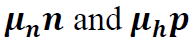
Drift Currents:
The mobile charges can move in the presence of an Electric Field E. This gives rise to drift Currents:
At room temperature (300K), for moderately doped silicon:

(electrons have higher mobility)
Drift currents give rise to ohmic losses,
are the respective conductivity.
Diffusion Currents:
The mobile charges can move and if there is a difference in concentration in the material, the mobile charge will diffuse to the region of lower concentration giving rise to a diffusion current:
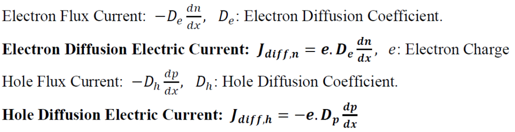
Einstein’s relation gives the relationship between the Diffusion and Mobility Coefficients:
Near Charge Neutrality Approximation:
In regions where many mobile charges are present (the bulk region), these charges will flow in such a way to ensure ‘near’ charge neutrality in such regions. The approximation is ‘near’ because if drift currents are flowing at different amounts, the Electric field (assuming same concentration of mobile charges) will differ at different regions, leading to some net charge at different regions.
PN Junction, Depletion layer and ‘Built in Potential’
The basic diode is made up of a PN junction.
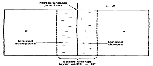
A PN Junction is formed when a semiconductor has a P region and an N region meeting.
This creates a layer at the boundary practically without mobile charges, but only the fix charges. This is the depletion layer (depleted of mobile charges). Its origin can be explained as follows:
The ‘N’ type semiconductor has a high concentration of electrons compared to the p-side. This electron concentration difference or gradient creates a diffusion current with electrons flowing to the p-side. This leaves the fixed ‘+’ charges at the N side of the junction. Likewise, the holes from the ‘P’ type diffuse to the ‘N’ side, leaving negative fixed charges. These are Diffusion currents.
The fixed charges in the depletion region create an electrical field or potential (with thus drift currents) that reverse the flow of the mobile charges (electrons & holes).
An equilibrium is reached when the deletion region’s potential difference build up sufficiently to create a drift current that cancels the diffusion current completely.


